- 您现在的位置:买卖IC网 > Sheet目录1918 > DSPIC33FJ32MC202-E/MM (Microchip Technology)IC DSPIC MCU/DSP 32K 28QFN
dsPIC33FJ32MC202/204 and dsPIC33FJ16MC304
DS70283K-page 14
2007-2012 Microchip Technology Inc.
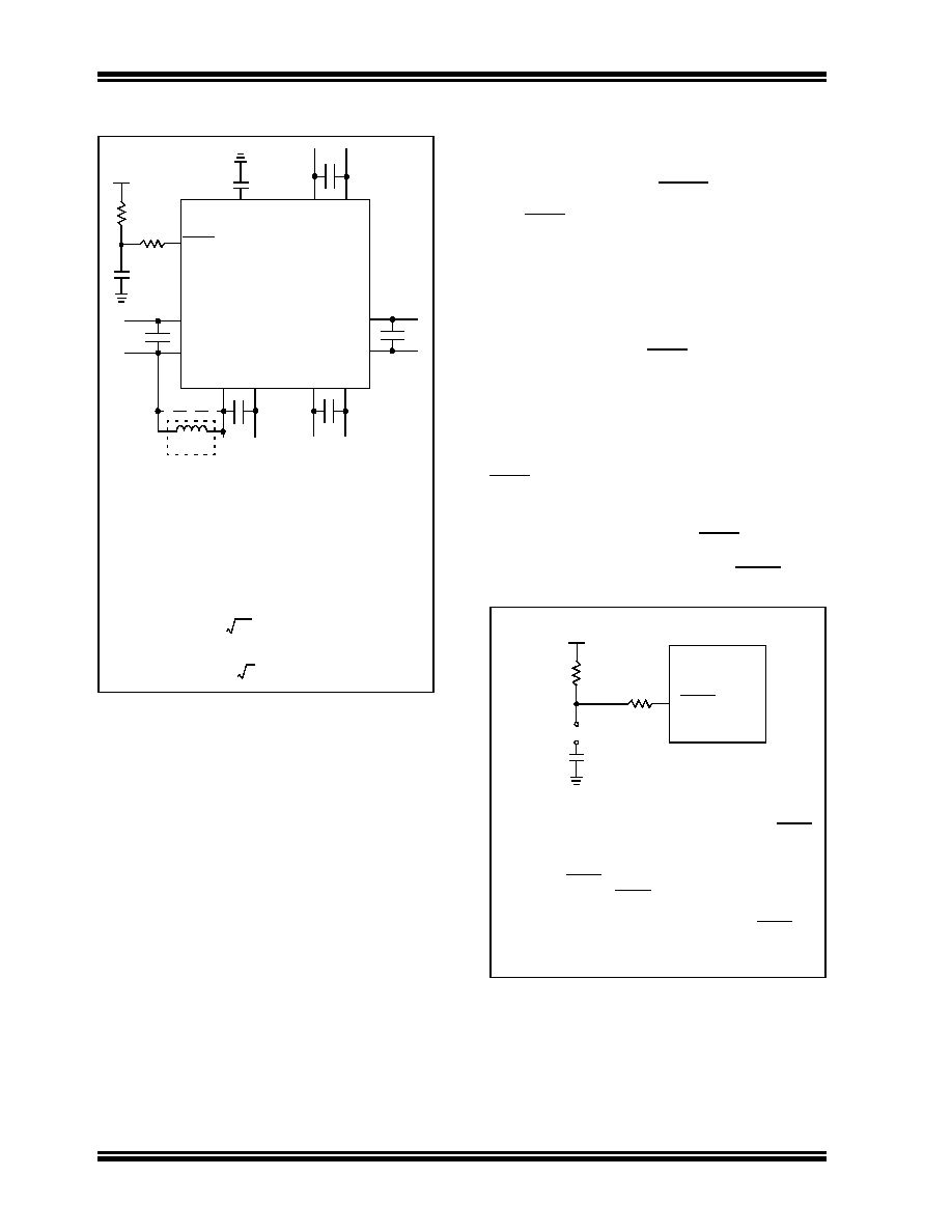
FIGURE 2-1:
RECOMMENDED
MINIMUM CONNECTION
2.2.1
TANK CAPACITORS
On boards with power traces running longer than six
inches in length, it is suggested to use a tank capacitor
for integrated circuits including DSCs to supply a local
power source. The value of the tank capacitor should
be determined based on the trace resistance that con-
nects the power supply source to the device, and the
maximum current drawn by the device in the applica-
tion. In other words, select the tank capacitor so that it
meets the acceptable voltage sag at the device. Typical
values range from 4.7 F to 47 F.
2.3
CPU Logic Filter Capacitor
Connection (VCAP)
A low-ESR (<5 Ohms) capacitor is required on the
VCAP pin, which is used to stabilize the voltage
regulator output voltage. The VCAP pin must not be
connected to VDD, and must have a capacitor between
4.7 F and 10 F, 16V connected to ground. The type
can be ceramic or tantalum. Refer to Section 24.0
for
additional
information.
The placement of this capacitor should be close to the
VCAP. It is recommended that the trace length not
exceed one-quarter inch (6 mm). Refer to Section 21.2
“On-Chip Voltage Regulator” for details.
2.4
Master Clear (MCLR) Pin
The MCLR pin provides for two specific device
functions:
Device Reset
Device programming and debugging
During device programming and debugging, the
resistance and capacitance that can be added to the
pin must be considered. Device programmers and
debuggers drive the MCLR pin. Consequently,
specific voltage levels (VIH and VIL) and fast signal
transitions must not be adversely affected. Therefore,
specific values of R and C will need to be adjusted
based on the application and PCB requirements.
For example, as shown in Figure 2-2, it is
recommended that capacitor C is isolated from the
MCLR pin during programming and debugging
operations.
Place the components shown in Figure 2-2 within
one-quarter inch (6 mm) from the MCLR pin.
FIGURE 2-2:
EXAMPLE OF MCLR PIN
CONNECTIONS
dsPIC33F
V
DD
V
SS
VDD
VSS
VDD
AV
DD
AV
SS
V
DD
V
SS
0.1 F
Ceramic
0.1 F
Ceramic
0.1 F
Ceramic
0.1 F
Ceramic
C
R
VDD
MCLR
0.1 F
Ceramic
V
CAP
L1(1)
R1
10 F
Tantalum
Note 1:
As an option, instead of a hard-wired connection, an
inductor (L1) can be substituted between VDD and
AVDD to improve ADC noise rejection. The inductor
impedance should be less than 1
Ω and the inductor
capacity greater than 10 mA.
Where:
f
FCNV
2
--------------
=
f
1
2
π LC
()
-----------------------
=
L
1
2
πfC
()
---------------------
2
=
(i.e., ADC conversion rate/2)
Note 1: R
≤ 10 kΩ is recommended. A suggested
starting value is 10 k
Ω. Ensure that the MCLR
pin VIH and VIL specifications are met.
2: R1
≤ 470W will limit any current flowing into
MCLR from the external capacitor C, in the
event of MCLR pin breakdown, due to Elec-
trostatic Discharge (ESD) or Electrical
Overstress (EOS). Ensure that the MCLR pin
VIH and VIL specifications are met.
C
R1(2)
R(1)
VDD
MCLR
dsPIC33F
JP
发布紧急采购,3分钟左右您将得到回复。
相关PDF资料
DSPIC33FJ64MC710-I/PF
IC DSPIC MCU/DSP 64K 100TQFP
EFM32G200F64
MCU 32BIT 64KB FLASH 32-QFN
EFM32G210F128
IC MCU 32BIT 128KB FLASH 32QFN
EFM32G222F64
IC MCU 32BIT 64KB FLASH QFP48
EFM32G230F128
IC MCU 32BIT 128KB FLASH 64QFN
EFM32G232F64
IC MCU 32BIT 64KB FLASH LQFP64
EFM32G280F64
MCU 32BIT 64KB FLASH 100-LQFP
EFM32G290F64
MCU 32BIT 64KB FLASH 112-BGA
相关代理商/技术参数
dsPIC33FJ32MC202-E/SO
功能描述:数字信号处理器和控制器 - DSP, DSC 16B DSC 28LD32KB Motor40 MIPS RoHS:否 制造商:Microchip Technology 核心:dsPIC 数据总线宽度:16 bit 程序存储器大小:16 KB 数据 RAM 大小:2 KB 最大时钟频率:40 MHz 可编程输入/输出端数量:35 定时器数量:3 设备每秒兆指令数:50 MIPs 工作电源电压:3.3 V 最大工作温度:+ 85 C 封装 / 箱体:TQFP-44 安装风格:SMD/SMT
dsPIC33FJ32MC202-E/SP
功能描述:数字信号处理器和控制器 - DSP, DSC 16B DSC 28LD32KB Motor40 MIPS RoHS:否 制造商:Microchip Technology 核心:dsPIC 数据总线宽度:16 bit 程序存储器大小:16 KB 数据 RAM 大小:2 KB 最大时钟频率:40 MHz 可编程输入/输出端数量:35 定时器数量:3 设备每秒兆指令数:50 MIPs 工作电源电压:3.3 V 最大工作温度:+ 85 C 封装 / 箱体:TQFP-44 安装风格:SMD/SMT
dsPIC33FJ32MC202-E/SS
功能描述:数字信号处理器和控制器 - DSP, DSC 16 bit DSC 40MIPS 32KB Flash RoHS:否 制造商:Microchip Technology 核心:dsPIC 数据总线宽度:16 bit 程序存储器大小:16 KB 数据 RAM 大小:2 KB 最大时钟频率:40 MHz 可编程输入/输出端数量:35 定时器数量:3 设备每秒兆指令数:50 MIPs 工作电源电压:3.3 V 最大工作温度:+ 85 C 封装 / 箱体:TQFP-44 安装风格:SMD/SMT
dsPIC33FJ32MC202-H/MM
功能描述:数字信号处理器和控制器 - DSP, DSC 16-bit 32KB Flash 40 MIPS RoHS:否 制造商:Microchip Technology 核心:dsPIC 数据总线宽度:16 bit 程序存储器大小:16 KB 数据 RAM 大小:2 KB 最大时钟频率:40 MHz 可编程输入/输出端数量:35 定时器数量:3 设备每秒兆指令数:50 MIPs 工作电源电压:3.3 V 最大工作温度:+ 85 C 封装 / 箱体:TQFP-44 安装风格:SMD/SMT
dsPIC33FJ32MC202-H/SO
功能描述:数字信号处理器和控制器 - DSP, DSC 16-bit 32KB Flash 40 MIPS RoHS:否 制造商:Microchip Technology 核心:dsPIC 数据总线宽度:16 bit 程序存储器大小:16 KB 数据 RAM 大小:2 KB 最大时钟频率:40 MHz 可编程输入/输出端数量:35 定时器数量:3 设备每秒兆指令数:50 MIPs 工作电源电压:3.3 V 最大工作温度:+ 85 C 封装 / 箱体:TQFP-44 安装风格:SMD/SMT
dsPIC33FJ32MC202-I/MM
功能描述:数字信号处理器和控制器 - DSP, DSC 16B DSC 28LD 32KB FlashMotor40 RoHS:否 制造商:Microchip Technology 核心:dsPIC 数据总线宽度:16 bit 程序存储器大小:16 KB 数据 RAM 大小:2 KB 最大时钟频率:40 MHz 可编程输入/输出端数量:35 定时器数量:3 设备每秒兆指令数:50 MIPs 工作电源电压:3.3 V 最大工作温度:+ 85 C 封装 / 箱体:TQFP-44 安装风格:SMD/SMT
DSPIC33FJ32MC202-I/MM
制造商:Microchip Technology Inc 功能描述:16 bit DSC 28LD 32KB Flash Motor 40 MIPS
DSPIC33FJ32MC202-I/MM
制造商:Microchip Technology Inc 功能描述:DSC 16BIT 32K FLASH 40MIPS 28QFN-S 制造商:Microchip Technology Inc 功能描述:DSC, 16BIT, 32K FLASH, 40MIPS, 28QFN-S